
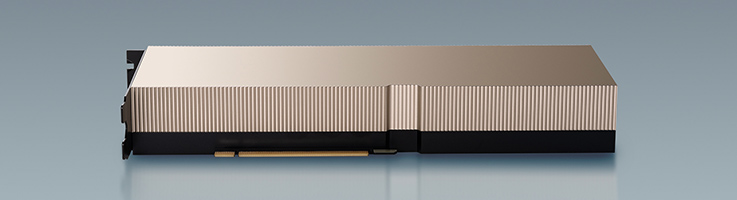
The NVIDIA® A100 Tensor Core GPU offers unprecedented acceleration at every scale and is accelerating the most important work of our time, powering the world’s highest-performing elastic data centers for AI, data analytics, and HPC. Powered by the NVIDIA Ampere architecture, A100 is the engine of the NVIDIA data center platform. A100 provides up to 20x higher performance over the prior generation and can be partitioned into seven GPU instances to dynamically adjust to shifting demands.
This blog gives you a deep dive inside the A100 GPU, and describes important new features of NVIDIA Ampere architecture GPUs.
The diversity of compute-intensive applications running in modern cloud data centers has driven the explosion of NVIDIA GPU-accelerated cloud computing. Such intensive applications include AI deep learning (DL) training and inference, data analytics, scientific computing, genomics, edge video analytics and 5G services, graphics rendering, cloud gaming, and many more. From scaling-up AI training and scientific computing, to scaling-out inference applications, to enabling real-time conversational AI, NVIDIA GPUs provide the necessary horsepower to accelerate numerous complex and unpredictable workloads running in today’s cloud data centers.
NVIDIA GPUs are the leading computational engines powering the AI revolution, providing tremendous speedups for AI training and inference workloads. In addition, NVIDIA GPUs accelerate many types of HPC and data analytics applications and systems, allowing you to effectively analyze, visualize, and turn data into insights. The NVIDIA accelerated computing platforms are central to many of the world’s most important and fastest-growing industries.
Overview of the NVIDIA A100 Tensor Core GPU
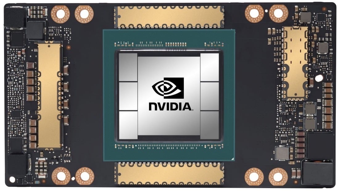
The NVIDIA A100 Tensor Core GPU is based on the new NVIDIA Ampere GPU architecture, and builds upon the capabilities of the prior NVIDIA Tesla V100 and V100S GPUs. It adds many new features and delivers significantly faster performance for HPC, AI, and data analytics workloads.
A100 provides strong scaling for GPU compute and DL applications running in single and multi-GPU workstations, servers, clusters, cloud data centers, systems at the edge, and supercomputers. The A100 GPU enables building elastic, versatile, and high throughput data centers.
The A100 GPU includes a revolutionary new Multi-Instance GPU (MIG) virtualization and GPU partitioning capability that is particularly beneficial to cloud service providers (CSPs). When configured for MIG operation, the A100 permits CSPs to improve the utilization rates of their GPU servers, delivering up to 7x more GPU Instances for no additional cost. Robust fault isolation allows them to partition a single A100 GPU safely and securely.
A100 adds a powerful new third-generation Tensor Core that boosts throughput over V100 or V100S while adding comprehensive support for DL and HPC data types, together with a new Sparsity feature that delivers a further doubling of throughput.
New TensorFloat-32 (TF32) Tensor Core operations in A100 provide an easy path to accelerate FP32 input/output data in DL frameworks and HPC, running 10x faster than V100 or V100S FP32 FMA operations or 20x faster with sparsity. For FP16/FP32 mixed-precision DL, the A100 Tensor Core delivers 2.5x the performance of V100 or V100S, increasing to 5x with sparsity.
New BFLOAT16 (BF16)/FP32 mixed-precision Tensor Core operations run at the same rate as FP16/FP32 mixed-precision. Tensor Core acceleration of INT8, INT4, and binary round out support for DL inferencing, with A100 sparse INT8 running 20x faster than V100 or V100S INT8. For HPC, the A100 Tensor Core includes new IEEE-compliant FP64 processing that delivers 2.5x the FP64 performance of V100 or V100S.
The NVIDIA A100 GPU is architected to not only accelerate large complex workloads, but also efficiently accelerate many smaller workloads. A100 enables building data centers that can accommodate unpredictable workload demand, while providing fine-grained workload provisioning, higher GPU utilization, and improved TCO.
The NVIDIA A100 GPU delivers exceptional speedups over V100 or V100S for AI training and inference workloads.
A100 GPU Streaming Multiprocessor
The new streaming multiprocessor (SM) in the NVIDIA Ampere architecture-based A100 Tensor Core GPU significantly increases performance, builds upon features introduced in both the Volta and Turing SM architectures, and adds many new capabilities.
The A100 third-generation Tensor Cores enhance operand sharing and improve efficiency, and add powerful new data types, including the following:
- TF32 Tensor Core instructions that accelerate processing of FP32 data
- IEEE-compliant FP64 Tensor Core instructions for HPC
- BF16 Tensor Core instructions at the same throughput as FP16
This table provides key performance specifications for the NVIDIA A100 Tensor Core GPU:
| Peak FP641 | 9.7 TFLOPS |
| Peak FP64 Tensor Core1 | 19.5 TFLOPS |
| Peak FP321 | 19.5 TFLOPS |
| Peak FP161 | 78 TFLOPS |
| Peak BF161 | 39 TFLOPS |
| Peak TF32 Tensor Core1 | 156 TFLOPS | 312 TFLOPS2 |
| Peak FP16 Tensor Core1 | 312 TFLOPS | 624 TFLOPS2 |
| Peak BF16 Tensor Core1 | 312 TFLOPS | 624 TFLOPS2 |
| Peak INT8 Tensor Core1 | 624 TOPS | 1,248 TOPS2 |
| Peak INT4 Tensor Core1 | 1,248 TOPS | 2,496 TOPS2 |
1Peak rates are based on the GPU boost clock. 2Effective TFLOPS/TOPS using the new Sparsity feature.
The new Sparsity support in A100 Tensor Cores can exploit fine-grained structured sparsity in DL networks to double the throughput of Tensor Core operations.
The larger and faster L1 cache and shared memory unit in A100 provides 1.5x the aggregate capacity per SM compared to V100 or V100S (192 KB vs. 128 KB per SM) to deliver additional acceleration for many HPC and AI workloads.
Several other new SM features improve efficiency and programmability and reduce software complexity.
40 GB HBM2e and 40 MB L2 Cache
To feed its massive computational throughput, the NVIDIA A100 GPU has 40 GB of high-speed HBM2e memory with a class-leading 1555 GB/sec of memory bandwidth—a 73% increase compared to Tesla V100 or V100S. In addition, the A100 GPU has significantly more on-chip memory including a 40 MB Level 2 (L2) cache—nearly 7x larger than V100 or V100S—to maximize compute performance. With a new partitioned crossbar structure, the A100 L2 cache provides 2.3x the L2 cache read bandwidth of V100 or V100S.
To optimize capacity utilization, the NVIDIA Ampere architecture provides L2 cache residency controls for you to manage data to keep or evict from the cache. A100 also adds Compute Data Compression to deliver up to an additional 4x improvement in DRAM bandwidth and L2 bandwidth, and up to 2x improvement in L2 capacity.
Multi-Instance GPU
The new Multi-Instance GPU (MIG) feature allows the A100 Tensor Core GPU to be securely partitioned into as many as seven separate GPU Instances for CUDA applications, providing multiple users with separate GPU resources to accelerate their applications.
With MIG, each instance’s processors have separate and isolated paths through the entire memory system. The on-chip crossbar ports, L2 cache banks, memory controllers, and DRAM address busses are all assigned uniquely to an individual instance. This ensures that an individual user’s workload can run with predictable throughput and latency, with the same L2 cache allocation and DRAM bandwidth, even if other tasks are thrashing their own caches or saturating their DRAM interfaces.
MIG increases GPU hardware utilization while providing a defined QoS and isolation between different clients, such as VMs, containers, and processes. MIG is especially beneficial for CSPs who have multi-tenant use cases. It ensures that one client cannot impact the work or scheduling of other clients, in addition to providing enhanced security and allowing GPU utilization guarantees for customers.
Third-generation NVIDIA NVLink
The third-generation of NVIDIA high-speed NVLink interconnect implemented in PCIe form factor A100 GPUs significantly enhances multi-GPU scalability, performance, and reliability. With more links per GPU, the new NVLink provides much higher GPU-GPU communication bandwidth, and improved error-detection and recovery features.
Third-generation NVLink has a data rate of 50 Gbit/sec per signal pair, nearly doubling the 25.78 Gbits/sec rate in the V100 or V100S. A single A100 NVLink provides 25-GB/second bandwidth in each direction similar to V100, but using only half the number of signal pairs per link compared to V100. The total number of links is increased to 12 in A100, vs. 6 in V100, yielding 600 GB/sec total bandwidth vs. 300 GB/sec for V100 or V100S.
Support for NVIDIA Magnum IO and Mellanox Interconnect Solutions
The A100 Tensor Core GPU is fully compatible with NVIDIA Magnum IO and Mellanox state-of-the-art InfiniBand and Ethernet interconnect solutions to accelerate multi-node connectivity.
The Magnum IO API integrates computing, networking, file systems, and storage to maximize I/O performance for multi-GPU, multi-node accelerated systems. It interfaces with CUDA-X libraries to accelerate I/O across a broad range of workloads, from AI and data analytics to visualization.
PCIe Gen 4 with SR-IOV
The A100 GPU supports PCI Express Gen 4 (PCIe Gen 4), which doubles the bandwidth of PCIe 3.0/3.1 by providing 31.5 GB/sec vs. 15.75 GB/sec for x16 connections. The faster speed is especially beneficial for A100 GPUs connecting to PCIe 4.0-capable CPUs, and to support fast network interfaces, such as 200 Gbit/sec InfiniBand.
A100 also supports single root input/output virtualization (SR-IOV), which allows sharing and virtualizing a single PCIe connection for multiple processes or VMs.
A100 Tensor Cores Accelerate HPC
The performance needs of HPC applications are growing rapidly. Many applications from a wide range of scientific and research disciplines rely on double precision (FP64) computations.
To meet the rapidly growing compute needs of HPC computing, the A100 GPU supports Tensor operations that accelerate IEEE-compliant FP64 computations, delivering up to 2.5x the FP64 performance of the NVIDIA Tesla V100 or V100S GPUs.
The new double precision matrix multiply-add instruction on A100 replaces eight DFMA instructions on Volta products, reducing instruction fetches, scheduling overhead, register reads, datapath power, and shared memory read bandwidth.
Each SM in A100 computes a total of 64 FP64 FMA operations/clock (or 128 FP64 operations/clock), which is twice the throughput of Tesla V100. The A100 Tensor Core GPU with 108 SMs delivers a peak FP64 throughput of 19.5 TFLOPS, which is 2.5x that of Tesla V100 or V100S.
With support for these new formats, the A100 Tensor Cores can be used to accelerate HPC workloads, iterative solvers, and various new AI algorithms.
| V100 | A100 | A100 Sparsity1 | |
| A100 FP16 vs. V100 FP16 | 31.4 TFLOPS | 78 TFLOPS | N/A |
| A100 FP16 TC vs. V100 FP16 TC | 125 TFLOPS | 312 TFLOPS | 624 TFLOPS |
| A100 BF16 TC vs. V100 or V100S FP16 TC | 125 TFLOPS | 312 TFLOPS | 624 TFLOPS |
| A100 FP32 vs. V100 FP32 | 15.7 TFLOPS | 19.5 TFLOPS | N/A |
| A100 TF32 TC vs. V100 FP32 | 15.7 TFLOPS | 156 TFLOPS | 312 TFLOPS |
| A100 FP64 vs. V100 FP64 | 7.8TFLOPS | 9.7 TFLOPS | N/A |
| A100 FP64 TC vs. V100 FP64 | 7.8 TFLOPS | 19.5 TFLOPS | N/A |
| A100 INT8 TC vs. V100 INT8 | 62 TOPS | 624 TOPS | 1248 TOPS |
| A100 INT4 TC | N/A | 1248 TOPS | 2496 TFLOPS |
| A100 Binary TC | N/A | 4992 TOPS | N/A |
1Effective TOPS/TFLOPS using the new Sparsity feature
A100 Introduces Fine-Grained Structures Sparsity
With the A100 GPU, NVIDIA introduces fine-grained structured sparsity, a novel approach that doubles compute throughput for deep neural networks.
Sparsity is possible in deep learning because the importance of individual weights evolves during the learning process, and by the end of network training, only a subset of weights have acquired a meaningful purpose in determining the learned output. The remaining weights are no longer needed.
Fine grained structured sparsity imposes a constraint on the allowed sparsity pattern, making it more efficient for hardware to do the necessary alignment of input operands. Because deep learning networks are able to adapt weights during the training process based on training feedback, NVIDIA engineers have found in general that the structure constraint does not impact the accuracy of the trained network for inferencing. This enables inferencing acceleration with sparsity.
For training acceleration, sparsity needs to be introduced early in the process to offer a performance benefit, and methodologies for training acceleration without accuracy loss are an active research area.
Combined L1 Data Cache and Shared Memory
First introduced in NVIDIA Tesla V100, the NVIDIA combined L1 data cache and shared memory subsystem architecture significantly improves performance, while also simplifying programming and reducing the tuning required to attain at or near-peak application performance. Combining data cache and shared memory functionality into a single memory block provides the best overall performance for both types of memory accesses.
The combined capacity of the L1 data cache and shared memory is 192 KB/SM in A100 vs. 128 KB/SM in V100 or V100S.
Simultaneous Execution of FP32 and INT32 Operations
Similar to V100, V100S, and Turing GPUs, the A100 SM also includes separate FP32 and INT32 cores, allowing simultaneous execution of FP32 and INT32 operations at full throughput, while also increasing instruction issue throughput.
Many applications have inner loops that perform pointer arithmetic (integer memory address calculations) combined with floating-point computations that benefit from simultaneous execution of FP32 and INT32 instructions. Each iteration of a pipelined loop can update addresses (INT32 pointer arithmetic) and load data for the next iteration while simultaneously processing the current iteration in FP32.
No Backplane Display Connectors
Because the A100 Tensor Core GPU is designed to be installed in high-performance servers and data center racks to power AI and HPC compute workloads, it does not include display connectors, NVIDIA RT Cores for ray tracing acceleration, or an NVENC encoder.
Conclusion
The NVIDIA A100 Tensor Core GPU delivers the next giant leap in NVIDIA’s accelerated data center platform, providing unmatched acceleration at every scale and enabling these innovators to do their life’s work in their lifetime. A100 powers numerous application areas including HPC, genomics, 5G, rendering, deep learning, data analytics, data science, and robotics.
Advancing the most important HPC and AI applications today—personalized medicine, conversational AI, and deep recommender systems—requires researchers, developers, and IT professionals to go big. A100 powers the NVIDIA data center platform that includes Mellanox HDR InfiniBand, NVSwitch, and the Magnum IO SDK for scaling up. This integrated suite of technologies efficiently scales to tens of thousands of GPUs to train the most complex AI networks at unprecedented speed.
The new MIG feature of the A100 GPU can partition each A100 into as many as seven GPU accelerators for optimal utilization, effectively improving GPU resource utilization and GPU access to more users and GPU-accelerated applications. With the A100 versatility, infrastructure managers can maximize the utility of every GPU in their data center to meet different-sized performance needs, from the smallest job to the biggest multi-node workload.
Make sure you register for NVIDIA GTC 21. This industry renowned event connects you with experts from NVIDIA to learn about the latest breakthroughs in AI, data center, accelerated computing, healthcare, intelligent networking, virtual reality, applications development and more. Attendance is free. Register today and enter for your chance to win a $25 Amazon gift card! Learn More: www.pny.com/gtc
For additional information visit PNY’s NVIDIA A100 product landing page or contact PNY at gopny@pny.com.


